
RC eNeM d.o.o.
Development of new production process for manufacturing of invisible interconnections from solutions of low-cost transparent conduction oxides by screen printing

About the company and the project impact
Slovenian company Development Centre RC eNeM Ltd. is working on the advancement of the research and development of new materials in various fields.
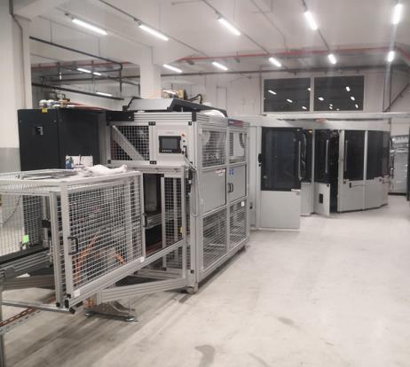
The conventional screen-printing method, which relies on the deposition of particles suspended in a solvent, is well developed and suitable for processing opaque materials but not for transparent coatings. Thus, there is an urgent need to develop an innovative technological process based on the deposition of the solution by screen printing, appropriate for the processing of transparent, sub-micrometre thick layers. Within this project, an economical, environmentally benign and solution-derived screen-printed process for manufacturing transparent interconnections on glass was implemented. The improvement of the manufacturing is reflected in the reduction of the production cost due to low-priced materials and low material consumption, in reduced reliance on raw materials, in particular, due to Al and Zn-salts availability and low quantities needed, and in the reduced generation of waste and pollution due to the electric-furnace curing, which contributed to the lower consumption of fossil fuels and reduction of CO2 emissions.
RC eNeM Ltd., Slovenia | www.rc-enem.siKET Technology
- Advanced Manufacturing
- Advanced Materials
Countries involved
- Slovenia
- Latvia
Outcome
The approach involves selecting low-cost metal oxides, processing solutions with appropriate properties for the screen printing, and optimisation of thin-films processing conditions to obtain electrically conductive and transparent layers. A successful thin-film fabrication was verified by microstructural and optoelectronic characterisation.
The solutions suitable for screen printing have been developed by modification of chemical composition and rheological properties of spin-coating solutions. The developed solution was successfully screen printed and cured on the industrial product bottle in the SME's production line. The solution-derived AZO thin films processed in an industrial environment have optical transmittance in the visible range higher than AZO films prepared by physical deposition methods. Its electrical performances are slightly lower than the ones of ZnO-based thin films prepared by chemical solution deposition methods, but those can be improved by modifying the processing conditions.
 layer screen printed on glass")

Key success factors
Besides the excellent collaboration between the SME and the KET TCs, the key success factor of the project is their interdisciplinary expert knowledge.
The realisation of such thin films has been feasible due to the KET TCs' experience in solution processing and tuning their properties for several technologies, experience in screen-printing technology, processing of thick and thin films on various substrates, expertise in optimisation of thin film's processing conditions, as well as expertise in several analytical methods for characterisation of solutions and thin films.
Corresponding KETs Technology Centre:
Josef Stefan Institute| Ljubljana, Slovenia
Institute of Solid State Physics, University of Latvia | Riga, Latvia